-
Phone
13761090949
-
Address
5th Floor, Helen International Building, 778 Baoshan Road, Hongkou District, Shanghai
Product Categories
Shanghai Juna Technology Co., Ltd
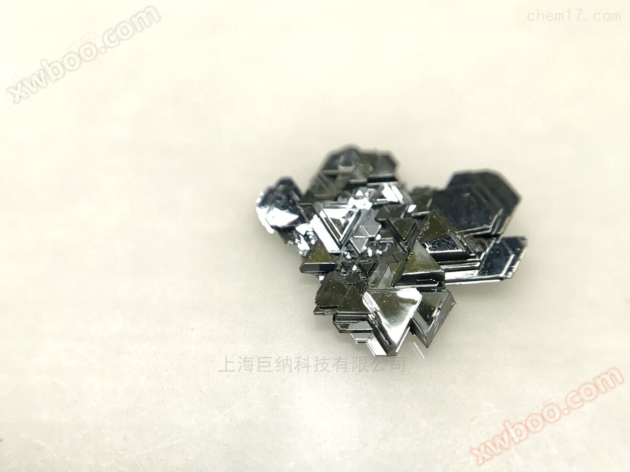
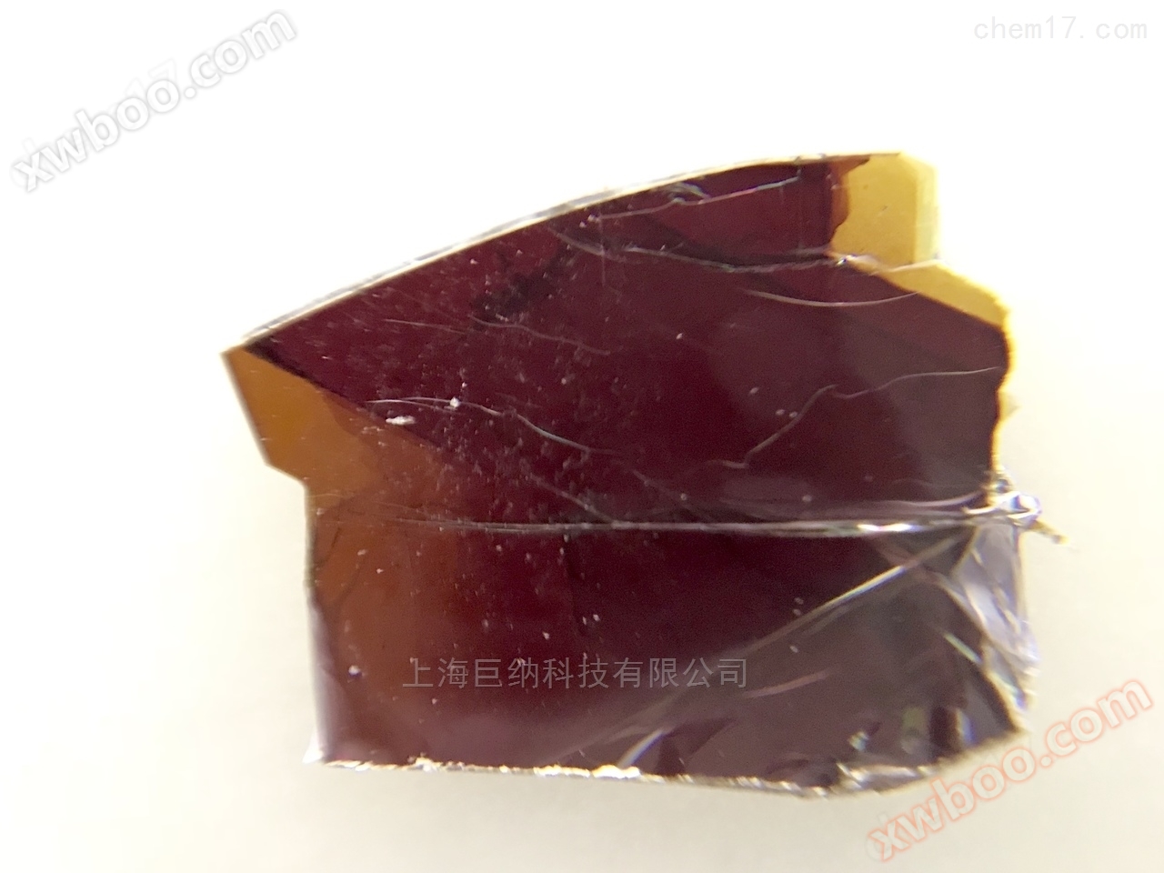
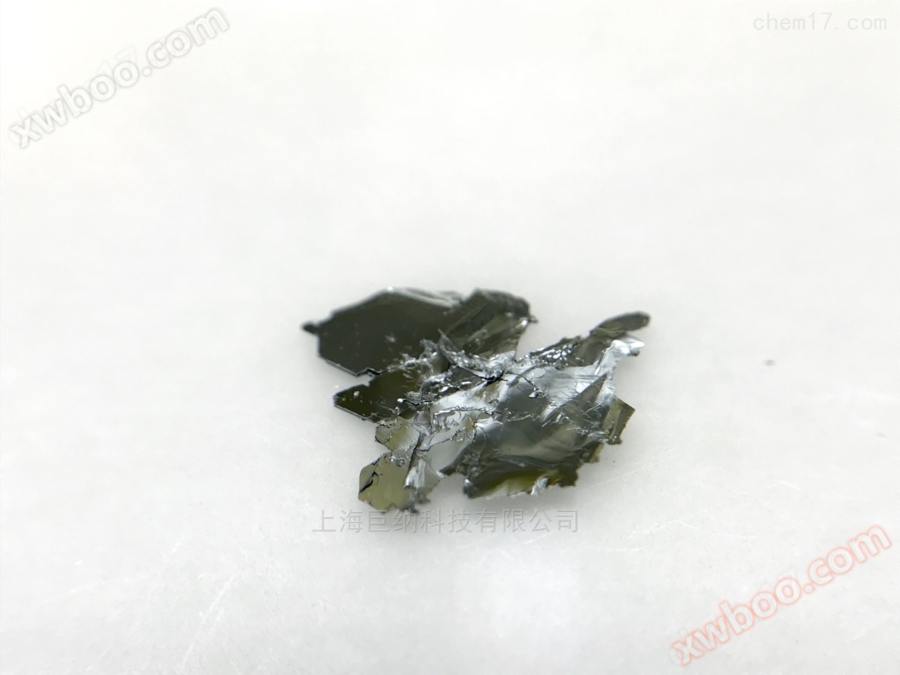
NbTe2 crystals, niobium telluride crystals
NegotiableUpdate on 06/23
- Model
- Nature of the Manufacturer
- Producers
- Product Category
- Place of Origin
Overview
简要描述:100% environmentally stable metallic NbTe2 crystals: In the bulk form, niobium ditelluride is metallic.
Product Details
100% environmentally stable metallic NbTe2 crystals: In the bulk form, niobium ditelluride is metallic. Similar to molybdenum disulfide, it has layered structure (lamellar) with weak interlayer coupling. NbTe2 displays metallic and superconducting behavior. Undergoes superconducting transition around 1.1 K in bulk, but predicted to higher for thinner sheets. Unlike other sources, our NbTe2 crystals are grown by defect and impurity free flux zone technique (see the comparison between chemical vapor transport [CVT] below). Clean and defect free nature enabled researchers to observe clean superconductivity, phase transitions, and perform quantum transport measurements with confidence in the crystal.
If your research needs atomically flat NbTe2 samples for scanning tunneling microscopy (STM) measurements please contact us.
Properties of NbTe2 crystals by 2Dsemiconductors USA

Growth method matters> Flux zone or CVT growth method? Contamination of halides and point defects in layered crystals are well known cause for their reduced electronic mobility, reduced anisotropic response, poor e-h recombination, low-PL emission, and lower optical absorption. Flux zone technique is a halide free technique used for synthesizing truly semiconductor grade vdW crystals. This method distinguishes itself from chemical vapor transport (CVT) technique in the following regard: CVT is a quick (~2 weeks) growth method but exhibits poor crystalline quality and the defect concentration reaches to 1E11 to 1E12 cm-2 range. In contrast, flux method takes long (~3 months) growth time, but ensures slow crystallization for perfect atomic structuring, and impurity free crystal growth with defect concentration as low as 1E9 - 1E10 cm-2. During check out just state which type of growth process is preferred. Unless otherwise stated, 2Dsemiconductors ships Flux zone crystals as a default choice.

Similar Product Recommend