- Phone
-
Address
Room 102, Building D, Jingmao International Apartment, Jingtong Expressway Exit, Chaoyang District, Beijing
Product Categories
Beijing Century Kexin Scientific Instrument Co., Ltd

Scanning tunneling microscope (teaching type) FM Nanoview T-STM
NegotiableUpdate on 02/05
- Model
- Nature of the Manufacturer
- Producers
- Product Category
- Place of Origin
Overview
Scanning tunneling microscope (teaching type) FM Nanoview T-STM
Product Details
◆Small and detachable design, very easy to carry and classroom teaching
◆The detection head and sample scanning table are integrated into one, with a very stable structure and strong anti-interference ability
◆Single axis drive sample automatically approaches the probe vertically, scanning the needle tip perpendicular to the sample
◆Intelligent needle insertion method for motor controlled automatic detection of piezoelectric ceramics, protecting probes and samples
◆sideCCDObservation system, real-time observation of probe insertion status and positioning of probe sample scanning area
◆Spring suspension shock-absorbing method, simple and practical, with good shock-absorbing effect
◆Integrated scanner non-linear correction user editor, with superior nano characterization and measurement accuracy98%
technical parameter
| Working mode | Constant high mode, constant current mode | Optical observation | 1-500x magnification continuously adjustable |
| Current spectrum curve | I-V curve, current distance curve | Scanning rate | 0.1Hz~62Hz |
| XY scanning range | 5×5um | Scanning angle | 0~360° |
| Z-scan range | 1um | Operating environment | Windows XP/7/8/10 operating system |
| Scanning resolution | Horizontal 0.05nm, vertical 0.01nm | communication interface | USB2.0/3.0 |
| Sample size | Φ≤68mm,H≤20mm | Shock absorption design | Spring suspension |
| Sample table itinerary | 15×15mm |
Application Cases

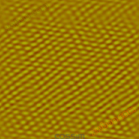

Graphite steps/Scanning range0.3µm×0.3µmHigh order graphite/Scanning range5nm×5nmGold cluster/Scanning range0.5µm×0.5µm
Similar Product Recommend