- Phone
-
Address
Room 501B, Building A, Science and Technology Building, No. 705 Yishan Road, Xuhui District, Shanghai
Product Categories
Ganwo Industrial (Shanghai) Co., Ltd

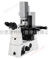
Parker Automation Industrial Atomic Force Microscope NX Wafer
NegotiableUpdate on 03/22
- Model
- Nature of the Manufacturer
- Producers
- Product Category
- Place of Origin
Overview
Park Systems Automated Industrial Atomic Force Microscope NX Wafer Instrument Type: Atomic Force Microscope Sample Stage Movement Range: 275mm * 200, 375mm * 300mm Sample Size: ≤ 300mm Positioning Detection Noise: ≤ 0.05nm
Product Details
Automated industrial grade atomic force microscope brings online chip inspection and measurement
Park Systems launches XE Wafer, a fully automated industrial grade atomic force microscope with the lowest noise in the industry. This automated atomic force microscope system is designed for sub meter level crystals (size 200) on all-weather production lines
Mm and 300
Mm) provides online high-resolution measurements of surface roughness, groove width, depth, and angle. With True
Non-Contact ™ Even in samples with soft structures, such as photoresist groove surfaces, XE Wafer can achieve non-destructive measurement.
Current issue
Currently, process engineers in the hard drive and semiconductor industries use expensive focused ion beams (FIB)/scanning electron microscopes (SEM) to obtain nanoscale surface roughness, sidewall angles, and heights. Unfortunately, FIB/SEM can damage the sample and is slow and costly.
Solution
The NX Wafer atomic force microscope enables fully automated online measurement of surface roughness, depth, and angle of 200 mm&300 mm crystals, with fast speed, high accuracy, and low cost.
benefit
NX Wafer enables non-destructive online imaging and enables direct, reproducible high-resolution measurements at multiple locations. The higher monitoring capability of * * degree and line width roughness allows process engineers to manufacture instruments with higher performance and significantly lower cost than FIB/SEM.
application
Crosstalk elimination achieves artifact free measurement
Unique decoupled XY axis scanning system provides a smooth scanning platform
Smooth linear XY axis scanning eliminates artifacts from background curvature**Distinctive features and industry-leading instrument statistical functions**Tool matchingCD(
Critical size

)
measurement
Outstanding * * and precise nano measurements not only improve efficiency, but also bring * high resolution and * low instrument sigma values to repeatability and reproducibility research.Precise nano measurementMeasurement of sub nanometer roughness of media and matrix
With the industry's lowest noise and True Non Contact
TM

XE Wafer achieves * * roughness measurement on * * smooth media and substrate samples.
**Angle measurement

The high-precision correction of Z-axis scanning orthogonality ensures that the angle measurement is less than 0.1 degrees.
Trench measurement

Unique TrueThe Non Contact mode is capable of non-destructive online measurement of corrosion details as small as 45 nm.
**Measurement of chemical mechanical polishing profile of through silicon via
With the help of low system noise and flat wheel profile scanning function, Park Systems has achieved * * * chemical mechanical polishing (TSV) for through silicon via holes
CMP contour measurement.
Park NX-Wafer
feature
Fully automatic graphic recognition
With the powerful high-resolution digital CCD lens and graphic recognition software, Park NX Wafer makes fully automatic graphic recognition and alignment possible.
Automatic measurement controlAutomation software makes the operation of NX Wafer effortless. The measurement program is optimized for cantilever tuning, scanning rate, gain, and point parameters, providing you with multi position analysis.True non-contact mode and longer probe lifespanThanks to Brick's high-strength Z-axis scanning system, the XE series atomic force microscope makes true non-contact mode possible. The true non-contact mode relies on the mutual attraction between atoms, rather than mutual repulsion.Therefore, in true non-contact mode, the distance between the probe and the sample can be maintained at a few nanometers, thereby covering the image quality of atomic force microscopy, ensuring the sharpness of the probe * *, and extending its service life.
Decoupled flexibility
XY
Axis and
Z
Axis scanner
The Z-axis scanner is completely decoupled from the XY axis scanner. The XY axis scanner moves the sample horizontally, while the Z-axis scanner moves the probe vertically. This setting enables smooth XY axis measurement, reducing out of plane movement to * low. In addition, the orthogonality and linearity of XY axis scanning are also excellent.
Low background noise in the industry
In order to detect small sample features and image flat surfaces, Park has launched a microscope with low industry background noise (<0.5A). The background noise is determined under the condition of "zero scan". When the cantilever comes into contact with the sample surface, measure the system noise under the following conditions:
·0 nm x 0 nm scanning range, stopping at one point
·0.5 gain, contact mode
·256 x 256 pixelsoptionHigh throughput automation
Automatic Probe Replacement (ATX)
With the automatic probe replacement function, the automatic measurement program can seamlessly connect. The system will automatically correct the position of the cantilever and optimize the measurement settings based on the reference graphic measurement data. **The magnetic probe replacement function has a success rate of up to 99%, which is higher than traditional vacuum technology.
Equipment front-end module
(EFEM)
Realize automatic crystal processing
Similar Product Recommend